Microelectronics Products and Services
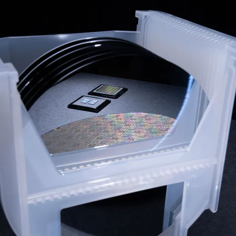
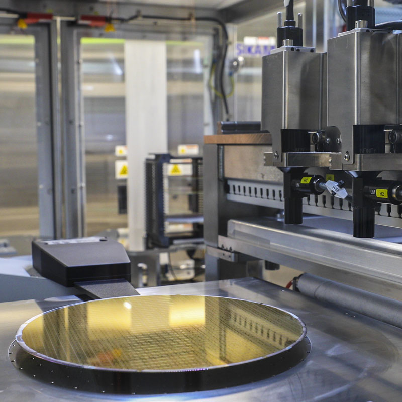
Northrop Grumman’s microelectronics products enable missions that range from advanced satellite communications and complex astrophysics systems to commercial applications, such as smartphones and ground-based communications infrastructure. Northrop Grumman has several U.S. based facilities with state-of-the-art design capabilities, multiple Si and III-V processing nodes, electrical testing, reliability screening, and failure analysis.
Products
Power Amplifiers
Power Amplifiers
Power Amplifiers
Part | Description | Frequency (GHz) | Gain (dB) | P1dB (dBm) | PSat (dBm) | Availability |
---|---|---|---|---|---|---|
APH668 | GaAs HEMT High Power Amplifier | 71 - 76 | 19 | TBD | 28 | Stock |
APH670 | GaAs HEMT Medium Power Amplifier | 71 - 76 | 21 | TBD | 25 | Stock |
APH667 |
GaAs HEMT High Power Amplifier | 81 - 86 | 17 | TBD | 25.5 | Stock |
APH669 | GaAs HEMT Medium Power Amplifier | 81 - 86 | 16 | 20 | 23.5 | Stock |
APH482 | HEMT High Power Amplifier | 92 - 96 | 7.5 | 22 | 25 | Stock |
APH631 | HEMT Power Amplifier | 92 - 96 | 23 | 15 | 18 | Stock |
APH635 | HEMT Power Amplifier | 92 - 95 | 17 | 20 | 22 | Stock |
GaN Power Amplifiers
Part | Description | Frequency (GHz) | Gain (dB) | P1dB (dBm) | Psat (dBm) | Form | Availability |
---|---|---|---|---|---|---|---|
APN267 | GaN HEMT Distributed Amplifier | 2-18 | 10 | 35 | 38 | Die | Stock |
APN270 | GaN HEMT Power Amplifier | 9-13.2 | 12 | 39 | 41 | Die | Stock |
APN252 | GaN HEMT Driver Amplifier | 10-14 | 25.5 | 34 | 38 | Die | Stock |
APN250 | GaN HEMT Power Amplifier | 10-14 | 13 | 39 | 42 | Die | Stock |
APN226 | GaN HEMT Power Amplifier | 13-16 | 20 | 36 | 39.5 | Die | Stock |
APN232 | GaN HEMT Power Amplifier | 13.5-15.5 | 13 | 38.5 | 42 | Die | Stock |
APN237 | GaN HEMT Dual Channel Power Amplifier | 13.5-15.5 | 12.5 | 40.5 | 44 | Die | Stock |
APN279 | GaN HEMT Power Amplifier | 16-20.8 | 17 | 39.5 | 42.5 | Die | Stock |
APN187 | GaN HEMT Power Amplifier | 17-22 | 17 | 40 | 42 | Die/Tab | Stock |
APN149 | GaN HEMT Power Amplifier | 18-23 | 20 | 38 | 39 | Die/Tab | Stock |
APN243 | GaN HEMT Power Amplifier | 23-28 | 20 | 38 | 40.5 | Die | Stock |
APN244 | GaN HEMT Power Amplifier | 23-28 | 21 | 37 | 39 | Die | Stock |
APN228 | GaN HEMT Power Amplifier | 27-31 | 16 | 39 | 41.2 | Die/Tab | Stock |
APN229 | GaN HEMT Power Amplifier | 27-32 | 20 | 17 | 39 | Die/Tab | Stock |
APN292 | GaN HEMT Power Amplifier | 27-30 | 20 | 42 | 45.5 | Die | Stock |
APN311 | GaN HEMT Power Amplifier | 27-31 | 20 | 43 | 45 | Die | Stock |
APN173 | GaN HEMT Power Amplifier | 34-36 | 19.5 | TBD | 37.5 | Die | Stock |
APN236 | GaN HEMT Power Amplifier | 34.5-35.5 | 16 | 38 | 40 | Die | Stock |
APN167 | GaN HEMT Power Amplifier | 43-46 | 20 | 35.5 | 38.5 | Die | Stock |
APN318 | GaN HEMT Power/Driver Amplifier | 47.2-51.4 | 15 | - | 40 | Die | Pre-Production |
APN319 | GaN HEMT Power/Driver Amplifier | 47.2-51.4 | 16 | - | 37 | Die | Pre-Production |
APN352 | GaN HEMT Power/Driver Amplifier | 47-51 | 15.5 | 40 | 40.5 | Die | Stock |
APN353 | GaN HEMT Power/Driver Amplifier | 47-51 | 14 | 37.5 | 39 | Die | Stock |
Low Noise Amplifiers
Part | Description | Frequency (GHz) | Gain (dB) | NF (dB) | P1dB (dBm) | Availability |
---|---|---|---|---|---|---|
ALP302_0 | InP HEMT Low Noise Amplifier | 17.2 - 21.2 | 33 | 0.8 | Stock | |
ALP302_A | InP HEMT Low Noise Amplifier | 17.2 - 21.2 | 32.5 | 0.8 | Stock | |
ALP291 | InP HEMT Low Noise Amplifier | 71 - 86 | 29 | 2.7 | 3 | Stock |
ALP275 | InP HEMT Low Noise Amplifier | 71 - 96 | > 26 | 3 | 4 | Stock |
ALP280 | InP HEMT Low Noise Amplifier | 80 - 100 | 29 | 2 | 3 | Stock |
ALP283 | InP HEMT Low Noise Amplifier | 80 - 100 | 29 | 2.5 | 3 | Stock |
ALH495 (-LN) | HEMT Low Noise Amplifier | 80 - 100 | 18 | 4.3 | 3 | Stock |
ALH495 (-GB) | HEMT Gain Block Amplifier | 80 - 100 | 18 | 4.8 | 3 | Stock |
ALH497 (-LN) | HEMT Low Noise Amplifier | 80 - 100 | 17 | 4.2 | 0 | Stock |
ALH497 (-GB) | HEMT Gain Block Amplifier | 80 - 100 | 17 | 4.9 | 0 | Stock |
ALH503 (-LN) | HEMT Low Noise Amplifier | 80 - 100 | 16 | 4.2 | 0 | Stock |
ALH503 (-GB) | HEMT Gain Block Amplifier | 80 - 100 | 16 | 4.9 | 0 | Stock |
ALH504 (-LN) | HEMT Low Noise Amplifier | 82 - 102 | 18 | 4.1 | 3 | Stock |
ALH504 (-GB) | HEMT Gain Block Amplifier | 82 - 102 | 18 | 4.8 | 3 | Stock |
ALP292 | InP HEMT Low Noise Amplifier | 90 - 112 | 30 | 3 | 3 | Stock |
ALH394 | HEMT Low Noise Amplifier | 92 - 96 | 17 | 5 | 5 | Stock |
Frequency Conversion
Mixers
Part | Description | RF Freq (GHz) | LO Freq (GHz) | IF Freq (GHz) | CL (dB) | Availability |
---|---|---|---|---|---|---|
MDJ183 | InP Schottky Diode Mixer | 17 - 32 | 17 - 32 | DC-10 | 8 | Pre-Production |
MDJ169 | InP Schottky Diode Mixer | 24 - 44 | 24 - 44 | DC-15 | 7.5 | Pre-Production |
MDJ178 | InP Schottky Diode Mixer | 37 - 61 | 37 - 61 | DC-15 | 8.5 | Pre-Production |
MDJ187 | InP Schottky Diode Mixer | 40 - 76 | 40 - 76 | DC-25 | 9 | Pre-Production |
MBH100 | HEMT Schottky Diode Mixer | 91 - 99 | 91 - 99 | DC-3 | 12 | Stock |
MDJ191 | InP Schottky Diode Mixer | 92 - 97 | 92 - 97 | DC-20 | 8.5 | Pre-Production |
Switches
Switches
Part | Description | Freq Out (GHz) | Freq In (GHz) | RF Input (dBm) | CG/CL/IL(dB) | Availability |
---|---|---|---|---|---|---|
SF0083 | SLCFET SPDT Switch | 0.5 – 25 | NA | NA | 0.38 / IL | Stock |
SDH148 | HEMT SPDT Switch | 80 - 100 | NA | NA | 3 / IL | Stock |
Modules
Modules
Part | Description | Frequency (GHz) | Gain (dB) | NF (dB) | P1dB (dBm) | Psat (dBm) | Form | Availability |
---|---|---|---|---|---|---|---|---|
MLA1101 | 140 GHz Low Noise Amplifier | 130-140 | 20 | 6 | TBD | TBD | Waveguide Module | Stock |
MGA2101 | 225-325 GHz Gain Block Module | 225-325 | 16 | 8 | TBD | 0 | Waveguide Module | Stock |
RAD Hard Mixed Signal
Discrete Devices
Discrete Devices
Datasheet | Description |
---|---|
Download | Bipolar RF Transistors |
Foundry Service
GaN HEMT
GaN HEMT
Technology | fT (GHz) | fmax (GHz) | Gm (mS/mm) | VDS,max (V) | Imax (A/mm) | Wafer Thickness (µm) | Airbridged Metal Available | Backside Vias | Wafer Size (mm) | Qualification |
---|---|---|---|---|---|---|---|---|---|---|
200 nm GaN HEMT | 60 | 150 | 325 | 24*/28** | 1.26 | 100 | Yes | Yes | 100 | Space Qualified |
150 nm GaN HEMT | 75 | 175 | 410 | 24 | 1.09 | 75 | Yes | Yes | 100 | Commercial Qualified |
90 nm GaN PWR HEMT | 100 | 200 | 650 | 20 | 1.55 | 50 | Yes | Yes | 100 | Commercial Qualification Expected Q4 2025 |
90 nm GaN HSLN HEMT | 100 | 200 | 730 | 10 | 1.5 | 50 | Yes | Yes | 100 | Commercial Qualification Expected Q1 2027 |
*Space, **Commercial
InP HEMT
InP HEMT
Technology | fT (GHz) | fmax (GHz) | Gm (mS/mm) | VDS,max (V) | Imax (A/mm) | Wafer Thickness (µm) | Airbridged Metal Available | Backside Vias | Wafer Size (mm) | Qualification |
---|---|---|---|---|---|---|---|---|---|---|
100 nm InP HEMT | 200 | 400 | 1200 | 1.2 | 0.9 | 75 | Yes | Yes | 100 | Space Qualified |
70 nm InP IACC | 250 | TBD | 2400 | 1.3 | 1.0 | 75 | Yes | Yes | 100 | Engineering |
35 nm InP IACC | 400 | 1100 | 2500 | 1.2 | 1.0 | 50 | Yes | Yes | 75 | Engineering |
25 nm InP IACC | 610 | 1500 | 3000 | 1.2 | 1.2 | 25 | Yes | Yes | 75 | Engineering |
GaAs HEMT
GaAs HEMT
Technology | fT (GHz) | fmax (GHz) | Gm (mS/mm) | VDS,max (V) | Imax (A/mm) | Wafer Thickness (µm) | Airbridged Metal Available | Backside Vias | Wafer Size (mm) | Qualification |
---|---|---|---|---|---|---|---|---|---|---|
150 nm GaAs HEMT | 90 | 200 | 565 | 5 | 0.68 | 50/100 | Yes | Yes | 100 | Space Qualified |
100 nm GaAs HEMT-Low Noise | 120 | 250 | 675 | 4 | 0.67 | 100 | Yes | Yes | 100 | Space Qualified |
100 nm GaAs HEMT-Power | 125 | 250 | 690 | 4 | 0.67 | 50/100 | Yes | Yes | 100 | Space Qualified |
InP HBT
InP HBT
Technology | fT (GHz) | fmax (GHz) | Beta | VCE,max (V) | Jc,max (mA/um²) | Wafer Thickness (µm) | Airbridged Metal Available | Backside Vias | Wafer Size (mm) | Qualification |
---|---|---|---|---|---|---|---|---|---|---|
0.65 um InP TF4 Digital (R445) | 150 | 400 | 70 | 6 | 1.5 | 75 | No | Yes | 100 | Engineering |
0.65 um InP TF4 Mixed-Signal (R442) | 250 | 300 | 70 | 3.5 | 2.5 | 75 | No | Yes | 100 | Space Qualified |
0.8 um InP TF2P Power (R447) | 75 | 150 | 70 | 7.5 | 0.75 | 75 | Yes | Yes | 100 | Engineering |
0.8 um InP TF2 Digital (R443) | 150 | 200 | 70 | 5 | 1.5 | 75 | Yes | Yes | 100 | Space Qualified |
0.25 um InP TF5 (R371P5) | 350 | 700 | 30 | 3 | 5 | 75 | No | Yes | 100 | Engineering |
SLCFET
SLCFET
Technology | Fco (THz) | Operation Frequency (GHz) | Ron (Ohm-mm) | Coff (pF/mm) | Ion (A/mm) | Control Voltage (V) | CW Input Power (dBm) | Vpo (V) | Breakdown Voltage (V) | Wafer Thickness (µm) | Airbridged Metal Available | Backside Vias | Wafer Size (mm) | Qualification |
SLCFET 3S | 1.8 | DC to 100 | 0.35 | 0.25 | 1.4 | 0, -14 | ≤ 35 | -5 | 40 | 100 | Yes | Yes | 100 | Engineering |
SLCFET 3HP | 1.8 | DC to 100 | 0.35 | 0.25 | 1.4 | 0, -20 | > 35 | -6 | 60 | 100 | Yes | Yes | 100 | Engineering |
Wafer Post Processing
Wafer Bumping and Dicing
- Bumping Process includes passivation, under bump metal, electroplating, solder sphere drop process.
- Whole Wafer probing 150mm to 300mm wafer sizes
- Dicing process includes: A dice before grind mechanical saw, thinning, laser die marking, die sort into waffle packs and tape & reel
- Metrology processing including whole wafer bump shear, 100% 2D/3D bump measurements as well as process controls in place for passivation and UBM layers
- Wafer sizes capability: 100mm, 150mm, 200mm and 300mm
Wafer Probe
Wafer Probe
Datasheet | Description |
---|---|
Download | Northrop Grumman’s Microelectronics Test Services |
Advanced Assembly Capabilities
- Multi-die, multi-foundry flip-chip 2D/3D assembly
- High accuracy thermocompression bonding
- Automated optical and x-ray inspections
- Organic, glass, silicon, and silicon carbide substrate handling
- Automated reflow, underfill, cleaning, ball attach
- High accuracy depaneling (mechanical, laser, saw)
- Spaceflight qualified packaging
- Hermetic wafer-level packaging
Advanced Test Capabilities
Test Capabilities Span Digital, Mixed Signal, Analog, and Cross-Domain
- Automated testing at multiple levels: whole wafer, singulated die on film frame, and package-level
- Multi-channel testing up to W-band
- Automated optical inspection (all formats)
- Classified testing options
- Post-test analysis & screening
Test Development Services
- Hardware & software design
- Test card, board, socket, etc. design
Reliability & Environmental Testing
- Burn-in / HAST / HTHB & other reliability tests
- RF shielded testing
Product Engineering & Management
- IP protection controls
- Yield management

Starry Nite Multi-project Wafer (MPW) Runs
Northrop Grumman was awarded the State-of-the-Art Radio Frequency Gallium Nitride (Starry Nite) program in Dec. 2021. As a part of the Starry Nite program, Northrop Grumman will mature a 90 nm Gallium Nitride node capable of W-band operation to manufacturing readiness level (MRL) 8. Throughout the program, foundry access to the 90 nm GaN node will be provided to external and internal designers through multi-project wafer (MPW) runs.
The 90 nm GaN technology is not a frozen process. Three model updates are planned during the program. Preliminary technology performance parameters are provided in the table.
Items of note:
- The Starry Nite program only pays for mask and fabrication
- Testing and subdicing available at additional cost
- ADS PDK supplied after NDA. Contact us for details on models for other design tools.
- Government purpose rights to the design may be required to participate
- All designs will be archived into a government repository
Starry Nite MPW Runs Calendar
STARRY NITE MPWs |
2025 |
||||||||||||||
Q1 | Q2 | Q3 | Q4 | ||||||||||||
Foundry | Process | Offering | Name | Jan | Feb | Mar | Apr | May | Jun | Jul | Aug | Sep | Oct | Nov | Dec |
NG |
GaN09 | 90nm | MPW1 | ||||||||||||
MPW2 | |||||||||||||||
MPW3 | |||||||||||||||
MPW4 | |||||||||||||||
MPW5 | |||||||||||||||
MPW7 | 11 | ||||||||||||||
MPW9 | 18 | ||||||||||||||
GaN09 +AIC | MPW6 | 31 | |||||||||||||
MPW8 | 2 | ||||||||||||||
GaN09-LN | MPW1-LN | 24 | |||||||||||||
MPW2-LN | 11 | ||||||||||||||
MPW1-M | 6 | 3 | 9 | ||||||||||||
MPW2-M | 27 | 25 | 3 | ||||||||||||
GaN09-LN +AIC | MPW3-M | 22 | 19 | 12 | |||||||||||
MPW4-M | 31 | 21 |
STARRY NITE MPWs |
2026 |
2027 |
|||||||||||||||||||||||||
Q1 | Q2 | Q3 | Q4 | Q1 | Q2 | Q3 | Q4 | ||||||||||||||||||||
Foundry | Process | Offering | Name | Jan | Feb | Mar | Apr | May | Jun | Jul | Aug | Sep | Oct | Nov | Dec | Jan | Feb | Mar | Apr | May | Jun | Jul | Aug | Sep | Oct | Nov | Dec |
NG |
GaN09 | 90nm | MPW1 | ||||||||||||||||||||||||
MPW2 | |||||||||||||||||||||||||||
MPW3 | |||||||||||||||||||||||||||
MPW4 | |||||||||||||||||||||||||||
MPW5 | |||||||||||||||||||||||||||
MPW7 | |||||||||||||||||||||||||||
MPW9 | |||||||||||||||||||||||||||
GaN09 +AIC | MPW6 | ||||||||||||||||||||||||||
MPW8 | 25 | ||||||||||||||||||||||||||
GaN09-LN | MPW1-LN | ||||||||||||||||||||||||||
MPW2-LN | |||||||||||||||||||||||||||
MPW1-M | 23 | ||||||||||||||||||||||||||
MPW2-M | 26 | ||||||||||||||||||||||||||
GaN09-LN +AIC | MPW3-M | 9 | |||||||||||||||||||||||||
MPW4-M | 20 | 15 |
The steps for the MPW runs are:
- Application deadline – Complete application form and submit by application deadline
- Performer space awarded – Government will use completed applications to decide on which designs to run on the mask and notify designers
- Design submission – Approved designs must be submitted by the submission date on the calendar
- Die delivered – At completion of fabrication, die will be delivered to designers
Email us if interested in participating in a Starry Nite MPW Run: as-mps.sales@ngc.com
Preliminary Technology Performance Parameters
Technology | fT (GHz) | fmax (GHz) | Gm (mS/mm) | VDS,max (V) | Imax (A/mm) | Wafer Thickness (µm) | Airbridged Metal Available | Backside Vias | Wafer Size (mm) |
---|---|---|---|---|---|---|---|---|---|
90 nm GaN PWR HEMT | 100 | 200 | 650 | 20 | 1.55 | 50 | Yes | Yes | 100 |
90 nm GaN HSLN HEMT | 100 | 200 | 730 | 10 | 1.5 | 50 | Yes | Yes | 100 |
Application Notes and Technical Papers
Application Notes
Application Notes
Revision | Title |
---|---|
Jun. 2008 | 94 GHz Chipset |
Apr. 2008 | 94 GHz Selector Guide |
Apr. 2008 | GaAs IC Die Handling, Assembly and Testing Techniques |
Apr. 2008 | Effects of Hydrogen on Hermetically Packaged GaAs MMICs |
May 2012 | GaN Chip Handling, Assembly and Testing Techniques |
Jun. 2024 | Die on Tab Datasheet |
Presentations
Presentations
Technical Papers
Technical Papers
Date | Forum | Title |
---|---|---|
2002 | GaAs MANTECH | GaAs Components for 60 GHz Wireless Communications Applications |
2001 | GaAs MANTECH | High-Reliability Deep Submicron GaAs Pseudomorphic HEMT MMIC Amplifiers |
1999 | IEEE RFIC Symposium | High Reliability Non-Hermetic 0.15 um GaAs Pseudomorphic HEMT MMIC Amplifiers |
Contact Us
Microelectronic Products and Services
Northrop Grumman Space Systems
One Space Park, D1/1024
Redondo Beach, CA 90278
USA
Sales Inquiries and Product Support: as-mps.sales@ngc.com