Home | Publications | Research | Team | Contact |


Fully 3D Printed RF StructureERFM

 
2019 PQE () 10-Jan-2019 V. Radisic and J. Tice


link


Polarization-independent, narrowband, near-IR spectral filters via guided mode resonances in ultrathin a-Si nanopillar arraysNP

 
ACS Photonics () 7-Jan-2019 Ryan Ng, Juan Garcia, Julia Greer

High spectral resolution plasmonic color filters with subwavelength dimensionsNP

 
ACS Photonics () 2-Jan-2019 Dagny Fleischman, Colton R. Bukowsky, Giulia Tagliabue, Luke A. Sweatlock, Harry A. Atwater

Capillary Wicking in Hierarchically Textured Copper Nanowire ArraysNano

 
ACS Applied Materials & Interfaces () 17-Dec-2018 J. Lee, Y. Suh, P.P. Dubey, M.T. Barako, Y. Won

Optimizing the Design of Composite Phase Change Materials for High Thermal Power DensityNano

 
Journal of Applied Physics () 10-Oct-2018 M.T. Barako, S. Lingamneni, J.S. Katz, T. Liu, K.E. Goodson, J. Tice

Broadband Electrically Tunable Dielectric Resonators Using Metal–Insulator TransitionsNP

 
ACS Photonics () 9-Sep-2018 Butakov NA, Knight MW, Lewi T, Iyer PP, Higgs D, Chorsi HT, Trastoy J, Granda JDel Valle, Valmianski I, Urban C, Kalcheim Y, Wang PY, § Hon PWC, Schuller IK, Schuller JA

Enhanced Capillary-Fed Boiling in Copper Inverse Opals via Template SinteringNano

 
Advanced Functional Materials () 21-Aug-2018 C. Zhang, J.W. Palko, M.T. Barako, M. Asheghi, J.G. Santiago, K.E. Goodson

Tailoring Permeability of Microporous Copper Structures through Template SinteringNano

 
ACS Applied Materials & Interfaces () 10-Aug-2018 C. Zhang, J.W. Palko, G. Rong, K.S. Pringle, M.T. Barako, T.J. Dusseault, M. Asheghi, J.G. Santiago, K.E.Goodson

Advancing semiconductor-electrocatalyst systems: application of surface transformation films and nanosphere lithographyNP

 
Faraday Discussions () 1-Aug-2018 Katharina Brinkert, Matthias Richter, Oemer Akay, Janine Liedtke, Michael Giersig, Han-Joachim Lewerenz

A fully-3D-printed complementary right/left-handed transmission lineERFM

 
IEEE Antennas and Propagation Symposium (2018) 13-Jul-2018 J. Hester, Evan Nguyen, R. Shishedo, J. Tice a full-3D design of a complementary right/left-handed (CRLH) transmission line structure with a transition frequency of 7.5GHz, which takes advantage of the unique capabilities of additive manufacturing technologies (AMT) is presented.

Efficient solar hydrogen generation in microgravity environmentNP

 
Nature Communications () 10-Jul-2018 Katharina Brinkert, Matthias Richter, Oemer Akay, Janine Liedtke, Michael Giersig, Han-Joachim Lewerenz

Heterogeneously Integrated V-Band AmplifierERFM

 
2018 IEEE International Microwave Symp. (2018) 12-Jul-2018 Dennis W. Scott, Eric Kaneshiro, K.K. Loi, Sujane Wang, Cedric Monier, and Augusto Gutierrez-Aitken We report on heterogeneously integrated V-band amplifier realized in four layer interconnect InP heterojunction bipolar transistor (HBT). The amplifier chiplet is integrated onto a passive InP carrier wafer with two layers of interconnect using heterogeneous integrated interconnects, which enable electrically short connection between two technologies. The heterogeneously integrated interconnect or transition has measured loss of £ 0.1 dB up to 30 GHz and ~0.4 dB at 90 GHz. Measured amplifier S-Parameters show almost no difference between before and after integration versions. Relatively flat output power between 11.5 and 12.5 dBm was demonstrated from 55 to 65 GHz. This is the first reported integration of V-band amplifier chiplets using heterogeneous integration, as well as lowest reported loss for heterogeneous interconnect transition.

Enhanced Heat Transfer using Microporous Copper Inverse OpalsNano

 
Journal of Electronic Packaging () 1-Jun-2018 H. Lee, T. Maitra, J. Palko, D. Kong, C. Zhang, M.T. Barako, Y.Won, M. Asheghi, K.E. Goodson

Experimental Characterization of Microfabricated Thermoelectric Energy Harvesters for Smart Sensor and Wearable ApplicationsNano

 
Adv. Mat. Tech. () 1-Jun-2018 M.T. Dunham, M.T. Barako, J.E. Cornett, Y. Gao, S. Haidar, N.Sun, M. Asheghi, B. Chen, K.E. Goodson

On the use of deep neural networks in optical communicationsQSM

 
Applied Optics () 20-May-2018 Erin M. Knutson, Matthew O'Donnell, Sean D. Huver, Ryan T. Glasser

Retrieval of all effective susceptibilities in nonlinear metamaterialsERFM

 
Physical Review A (2018) 30-Apr-2018 Stéphane Larouche and Vesna Radisic Electromagnetic metamaterials offer a great avenue to engineer and amplify the nonlinear response of materials. Their electric, magnetic, and magneto-electric linear and nonlinear response are related to their structure, providing unprecedented liberty to control those properties. Both the linear and the nonlinear properties of metamaterials are typically anisotropic. While the methods to retrieve the effective linear properties are well established, existing nonlinear retrieval methods have serious limitations. In the present work, we generalize a nonlinear transfer matrix approach to account for all nonlinear susceptibility terms and show how to use this approach to retrieve all effective nonlinear susceptibilities of metamaterial elements. The approach is demonstrated using sum frequency generation, but can be applied to other second order or higher order processes.

Additive Manufacturing for Full 3D RF StructuresERFM

 
GOMAC Tech 2018 (2018) 1-Mar-2018 Jimmy Hester, Evan Nguyen, Jesse Tice, Vesna Radisic In this paper, the authors introduce a promising fully-additive manufacturing approach for the fabrication of full-3D RF and mm-wave components and systems. The process, a combination of the stereolithography (SLA) printing of 3D dielectrics and the conformal aerosol-jet-printing of conductive traces, is introduced and benchmarked. A unique “roller coaster” electromagnetic-bandgap (EBG) 3D microstrip transmission line is proposed, fabricated and demonstrated.

Printable Materials for the Realization of High Performance RF Components: Challenges and OpportunitiesNano

 
International Journal of Antennas and Propagation (2018) 28-Jan-2018 Eva Rosker, Rajinder Sandhu, Jimmy Hester, Mark Goorsky, and Jesse Tice This review discusses the challenges facing low loss RF components, which has mostly been material limited by the robustness of the metal and the availability of AM-compatible dielectrics. We summarize the effective printing methods, review ink formulation, and the postprint processing steps necessary for targeted RF properties. We then detail the structure-property relationships critical to obtaining enhanced conductivities necessary for printed RF passive components. Finally, we give examples of demonstrations for various types of printed RF components and provide an outlook on future areas of research that will require multidisciplinary teams from chemists to RF system designers to fully realize the potential for printed RF components.

The risk-sensitive coverage problem: Multi-robot routing under uncertainty with service level and survival constraintsCA

 
Proceedings of the IEEE Conference on Decision and Control (2018) 23-Jan-2018 Stefan Jorgensen, Robert Chen, Mark Milam, Marco Pavone Consider a scenario where robots traverse a graph, but crossing each edge bears a risk of failure. A team operator seeks a set of paths for the smallest team which guarantee the probabilities that at least one robot visits each node satisfy specified per-node visit thresholds, and the probabilities each robot reaches its destination satisfy a per-robot survival threshold. We present the Risk-Sensitive Coverage (RSC) problem formally as an instance of the submodular set cover problem and propose an efficient cost-benefit greedy algorithm for finding a feasible set of paths. We prove that the number of robots deployed by our algorithm is no more than (λ/ps)(1 + log(λΔκ/ps)) times the smallest team, where Δκ quantifies the relative benefit of the first and last paths, ps is the per-robot survival probability threshold and 1/λ ≤ 1 is the approximation factor of an oracle routine for the well-known orienteering problem. We demonstrate the quality of our solutions by comparing to optimal solutions computed for special cases of the RSC and the efficiency of our approach by applying it to a search and rescue scenario where 225 sites must be visited, each with probability at least 0.95.

An SMT-based approach to secure state estimation under sensor and actuator attacksCA

 
Proceedings of the IEEE Conference on Decision and Control (2018) 23-Jan-2018 Mehrdad Showkatbakhsh, Yasser Shoukry, Robert H. Chen, Suhas Diggavi, Paulo Tabuada This paper addresses the problem of state estimation of a linear time-invariant system when some of the sensors or/and actuators are under adversarial attack. In our set-up, the adversarial agent attacks a sensor (actuator) by manipulating its measurement (input), and we impose no constraint on how the measurements (inputs) are corrupted. We introduce the notion of “sparse strong observability” to characterize systems for which the state estimation is possible, given bounds on the number of attacked sensors and actuators. Furthermore, we develop a secure state estimator based on Satisfiability Modulo Theory (SMT) solvers.

Optical magnetism in planar metamaterial heterostructuresNESD

 
Nature Communications (2018) 18-Jan-2018 Georgia T. Papadakis, Dagny Fleischman, Artur Davoyan, Pochi Yeh, Harry A. Atwater Harnessing artificial optical magnetism has previously required complex two- and three-dimensional structures, such as nanoparticle arrays and split-ring metamaterials. By contrast, planar structures, and in particular dielectric/metal multilayer metamaterials, have been generally considered non-magnetic. Although the hyperbolic and plasmonic properties of these systems have been extensively investigated, their assumed non-magnetic response limits their performance to transverse magnetic (TM) polarization. We propose and experimentally validate a mechanism for artificial magnetism in planar multilayer metamaterials. We also demonstrate that the magnetic properties of high-index dielectric/metal hyperbolic metamaterials can be anisotropic, leading to magnetic hyperbolic dispersion in certain frequency regimes. We show that such systems can support transverse electric polarized interface-bound waves, analogous to their TM counterparts, surface plasmon polaritons. Our results open a route for tailoring optical artificial magnetism in lithography-free layered systems and enable us to generalize the plasmonic and hyperbolic properties to encompass both linear polarizations.

Dielectric Barrier Layers by Low-Temperature Plasma-Enhanced Atomic Layer Deposition of Silicon DioxideNano

 
Thin Solid Films () 16-Jan-2018 M.T. Barako, T.S. English, S.Roy-Panzer, T.W Kenny, K.E. Goodson

Reconfigurable Composite Right/Left-Handed MetamaterialERFM

 
IEEE Radio and Wireless Symposium (2018) 15-Jan-2018 S. Larouche, X. Lan, E. Kaneshiro, A. Gutierrez-Aitken, and V. Radisic We report on a reconfigurable composite right/left-handed (CRLH) transmission line (TL) using an InP HBT fabrication process. A four unit cell- TL design is realized with distributed capacitors and inductors with each unit cell featuring a Schottky diode that is used to control the left-handed wave propagation in the structure.

Bright Breathers in Nonlinear Left-Handed Metamaterial LatticesERFM

 
Physical Scripta (2018) 8-Jan-2018 V Koukouloyannis, P G Kevrekidis, G P Veldes, D J Frantzeskakis, D DiMarzio, X Lan and V Radisic In the present work, we examine a prototypical model for the formation of bright breathers in nonlinear left-handed metamaterial lattices. Utilizing the paradigm of nonlinear transmission lines, we build a relevant lattice and develop a quasi-continuum multiscale approximation that enables us to appreciate both the underlying linear dispersion relation and the potential for bifurcation of nonlinear states. We focus here, more specifically, on bright discrete breathers which bifurcate from the lower edge of the linear dispersion relation at wavenumber k=pi. Guided by the multiscale analysis, we calculate numerically both the stable inter-site centered and the unstable site-centered members of the relevant family. We quantify the associated stability via Floquet analysis and the Peierls-Nabarro barrier of the energy difference between these branches. Finally, we explore the dynamical implications of these findings towards the potential mobility or lack thereof (pinning) of such breather solutions.

(Editor's Pick) High Breakdown Electric Field in b-Ga2O3/graphene vertical barristor heterostructureNano

 
Applied Physics Letters (2018) 1-Jan-2018 X Yan, I Esqueda, J Ma, J Tice, H Wang

The Team Surviving Orienteers problem: routing teams of robots in uncertain environments with survival constraintsCA

 
Autonomous Robots (2017) 27-Dec-2017 Stefan Jorgensen, Robert H. Chen, Mark B. Milam, Marco Pavone We study the following multi-robot coordination problem: given a graph, where each edge is weighted by the probability of surviving while traversing it, find a set of paths for K robots that maximizes the expected number of nodes collectively visited, subject to constraints on the probabilities that each robot survives to its destination. We call this the Team Surviving Orienteers (TSO) problem, which is motivated by scenarios where a team of robots must traverse a dangerous environment, such as aid delivery after disasters. We present the TSO problem formally along with several variants, which represent “survivability-aware” counterparts for a wide range of multi-robot coordination problems such as vehicle routing, patrolling, and informative path planning. We propose an approximate greedy approach for selecting paths, and prove that the value of its output is within a factor 1−e −p s /λ 1−e−ps/λ of the optimum where p s ps is the per - robot survival probability threshold, and 1 / λ≤1 1 / λ≤1 is the approximation factor of an oracle routine for the well-known orienteering problem.We also formalize an on - line update version of the TSO problem, and a generalization to heterogeneous teams where both robot types and paths are selected.We provide numerical simulations which verify our theoretical findings, apply our approach to real-world scenarios, and demonstrate its effectiveness in large - scale problems with the aid of a heuristic for the orienteering problem.

The matroid team surviving orienteers problem: Constrained routing of heterogeneous teams with risky traversalCA

 
Proceedings of the IEEE/RSJ Conference on Intelligent Robots and Systems (2017) 14-Dec-2017 Stefan Jorgensen, Robert Chen, Mark Milam, Marco Pavone Consider a setting where robots must visit sites represented as nodes in a graph, but each robot may fail when traversing an edge. The goal is to find a set of paths for a team of robots which maximizes the expected number of nodes collectively visited, while guaranteeing that the paths satisfy a notion of “independence” formalized by a matroid (e.g. limits on team size, number of visits to regions), and that the probabilities that each robot survives to its destination are above a given threshold. We call this problem the Matroid Team Surviving Orienteers (MTSO) problem, which has broad applications such as environmental monitoring in risky regions and search and rescue in dangerous conditions. We present the MTSO formally and detail numerous examples of matroids in a path planning context. We then propose an approximate greedy algorithm for selecting a feasible set of paths and prove that the value of the output is within a factor ps/ps + λ of the optimum, where ps is the per-robot survival probability threshold and 1/λ ≤ 1 is the approximation factor of an oracle routine for the well known orienteering problem. We demonstrate the efficiency of our approach by applying it to a scenario where a team of robots must gather information while avoiding pirates in the Coral Triangle.

Dense Aligned Copper Nanowire Composites as High Performance Thermal Interface MaterialsNano

 
ACS Applied Materials & Interfaces (2017) 9-Nov-2017 Michael T. Barako, Scott G. Isaacson, Feifei Lian, Eric Pop, Reinhold H. Dauskardt, Kenneth E. Goodson, and Jesse Tice

Hyper-selective plasmonic color filtersNP

 
Optics Express (2017) 30-Oct-2017 Dagny Fleischman, Luke A. Sweatlock, Hirotaka Murakami, and Harry Atwater The subwavelength mode volumes of plasmonic filters are well matched to the small size of state-of-the-art active pixels in CMOS image sensor arrays used in portable electronic devices. Typical plasmonic filters exhibit broad (> 100 nm) transmission bandwidths suitable for RBG or CMYK color filtering. Dramatically reducing the peak width of filter transmission spectra would allow for the realization of CMOS image sensors with multi- and hyperspectral imaging capabilities. We find that the design of 5 layer metal-insulator-metal-insulator-metal structures gives rise to multi-mode interference phenomena that suppress spurious transmission features and give rise to single transmission bands as narrow as 17 nm. The transmission peaks of these multilayer slot-mode plasmonic filters (MSPFs) can be systematically varied throughout the visible and near infrared spectrum, leading to a filter that is CMOS integrable, since the same basic MSPF structure can operate over a large range of wavelengths. We find that MSPF filter designs that can achieve a bandwidth less than 30 nm across the visible and demonstrate experimental prototypes with a FWHM of 70 nm, and we describe how experimental structure can be made to approach the limits suggested by the model.

Atomically Thin Femtojoule Memristive DeviceNano

 
Advanced Materials (2017) 25-Oct-2017 Huan Zhao, Zhipeng Dong, He Tian, Don DiMarzio, Myung-Geun Han, Lihua Zhang, Xiaodong Yan, Fanxin Liu, Lang Shen, Shu-Jen Han, Steve Cronin, Wei Wu, Jesse Tice, Jing Guo, Han Wang The morphology and dimension of the conductive filament formed in a memristive device are strongly influenced by the thickness of its switching medium layer. Aggressive scaling of this active layer thickness is critical toward reducing the operating current, voltage, and energy consumption in filamentary-type memristors. Previously, the thickness of this filament layer has been limited to above a few nanometers due to processing constraints, making it challenging to further suppress the on-state current and the switching voltage. Here, the formation of conductive filaments in a material medium with sub-nanometer thickness formed through the oxidation of atomically thin two-dimensional boron nitride is studied. The resulting memristive device exhibits sub-nanometer filamentary switching with sub-pA operation current and femtojoule per bit energy consumption. Furthermore, by confining the filament to the atomic scale, current switching characteristics are observed that are distinct from that in thicker medium due to the profoundly different atomic kinetics. The filament morphology in such an aggressively scaled memristive device is also theoretically explored. These ultralow energy devices are promising for realizing femtojoule and sub-femtojoule electronic computation, which can be attractive for applications in a wide range of electronics systems that desire ultralow power operation.

A Novel 3D-Printing-Enabled “Roller Coaster” Transmission LineERFM

 
IEEE Antennas and Propagation Symposium (2017) 19-Oct-2017 Jimmy Hester, Evan Nguyen, Jesse Tice, Vesna Radisic A novel transmission line design, which takes advantage of the unique manufacturing capabilities of additive-manufacturing technologies (AMTs), is introduced. The “roller coaster” transmission line, with a thickness and width-modulated microstrip line, displays an expected electromagnetic bandgap (EBG) and an additional simulated 43dB rejection than its 2D counterpart.

Thermal homeostasis using microstructured phase-change materialsNP

 
Optica (2017) 11-Oct-2017 Shao-Hua Wu, Mingkun Chen, Michael T. Barako, Vladan Jankovic, Philip W.C. Hon, Luke A. Sweatlock, and Michelle L. Povinelli Humans and other warm-blooded mammals maintain their body temperature within a narrow range in a process called homeostasis. This ability to maintain an internal temperature, which is relatively insensitive to changes in the external environment or heat load is vital for all complex processes that sustain life. Without the ability to regulate temperature, materials and devices that experience large temperature gradients or temperature cycles are vulnerable to performance degradation or even catastrophic failure. Thermal control akin to the way living organisms achieve thermal homeostasis is particularly important in environments such as space, where changing solar illumination can cause large temperature variations. Various systems have been used to mitigate temperature fluctuations; however, they tend to be bulky and require power. Here, we model micropatterned phase-change materials to design an efficient, solid-state alternative, which requires no external input power. Our design is based on switchable thermal emission, which takes advantage of temperature-induced phase-change behavior in thin films of vanadium oxide on silicon microcones.

Mapping Photoemission and Hot-Electron Emission from Plasmonic NanoantennasNP

 
Nano Letters (2017) 19-Sep-2017 Richard G. Hobbs, William P. Putnam, Arya Fallahi, Yujia Yang, Franz X. Kaertner, Karl K. Berggren

Microscale Liquid Transport in Polycrystalline Inverse Opals across Grain BoundariesNano

 
Scientific Reports (2017) 5-Sep-2017 Q. N. Pham, M. T. Barako, J. Tice & Y. Won Delivering liquid through the void spaces in porous metals is a daunting challenge for a variety of emerging interface technologies ranging from battery electrodes to evaporation surfaces. Hydraulic transport characteristics of well-ordered porous media are governed by the pore distribution, porosity, and morphology. Much like energy transport in polycrystalline solids, hydraulic transport in semi-ordered porous media is predominantly limited by defects and grain boundaries. Here, we report the wicking performances for porous copper inverse opals having pore diameters from 300 to 1000 nm by measuring the capillary-driven liquid rise. The capillary performance parameter within single crystal domain (K ij /R eff  = 10−3 to 10−2 µm) is an order of magnitude greater than the collective polycrystal (K eff /R eff  = ~10−5 to 10−3 µm) due to the hydraulic resistances (i.e. grain boundaries between individual grains). Inspired by the heterogeneity found in biological systems, we report that the capillary performance parameter of gradient porous copper (K eff /R eff  = ~10−3 µm), comparable to that of single crystals, overcomes hydraulic resistances through providing additional hydraulic routes in three dimensions. The understanding of microscopic liquid transport physics through porous crystals and across grain boundaries will help to pave the way for the spatial design of next-generation heterogeneous porous media.

Density matrix modeling of quantum cascade lasers without an artificially localized basis: A generalized scattering approachNSD

 
PRB (2017) 23-Aug-2017 Andrew Pan, Benjamin A. Burnett, Chi On Chui, and Benjamin S. Williams We derive a density matrix (DM) theory for quantum cascade lasers (QCLs) that describes the influence of scattering on coherences through a generalized scattering superoperator. The theory enables quantitative modeling of QCLs, including localization and tunneling effects, using the well-defined energy eigenstates rather than the ad hoc localized basis states required by most previous DM models. Our microscopic approach to scattering also eliminates the need for phenomenological transition or dephasing rates. We discuss the physical interpretation and numerical implementation of the theory, presenting sets of both energy-resolved and thermally averaged equations, which can be used for detailed or compact device modeling. We illustrate the theory's applications by simulating a high performance resonant-phonon terahertz (THz) QCL design, which cannot be easily or accurately modeled using conventional DM methods. We show that the theory's inclusion of coherences is crucial for describing localization and tunneling effects consistent with experiment.

Vertical Charge Transport and Negative Transconductance in Multilayer Molybdenum DisulfidesNSD

 
Nano Letters (2017) 20-Aug-2017 Vincent Gambin, Yuan Liu, Jian Guo Qiyuan He, Hao Wu, Hung-Chieh Cheng, Mengning Ding, Yu Huang and Xiangfeng Duan Negative transconductance (NTC) devices have been heavily investigated for their potential in low power logical circuit, memory, oscillating, and high-speed switching applications. Previous NTC devices are largely attributed to two working mechanisms: quantum mechanical tunneling, and mobility degradation at high electrical field. Herein we report a systematic investigation of charge transport in multilayer two-dimensional semiconductors (2DSCs) with optimized van der Waals contact and for the first time demonstrate NTC and antibipolar characteristics in multilayer 2DSCs (such as MoS2, WSe2). By varying the measurement temperature, bias voltage, and body thickness, we found the NTC behavior can be attributed to a vertical potential barrier in the multilayer 2DSCs and the competing mechanisms between intralayer lateral transport and interlayer vertical transport, thus representing a new working mechanism for NTC operation. Importantly, this vertical potential barrier arises from inhomogeneous carrier distribution in 2DSC from the near-substrate region to the bulk region, which is in contrast to conventional semiconductors with homogeneous doping defined by bulk dopants. We further show that the unique NTC behavior can be explored for creating frequency doublers and phase shift keying circuits with only one transistor, greatly simplifying the circuit design compared to conventional technology.

On-Chip Ultra-High‑Q Silicon Oxynitride Optical ResonatorsNSD

 
ACS Photonics (2017) 14-Aug-2017 Dongyu Chen, Andre Kovach, Xiaoqin Shen, Sumiko Poust, Andrea Armani Ultra-high quality (UHQ) optical resonators have enabled many fundamental scientific studies and advanced integrated photonic devices. Here, we developed silicon oxynitride UHQs which are substantially more robust to environmental degradation than today's state of the art silica devices.

W-Band InP HBT Power AmplifiersERFM

 
IEEE Microwave and Components Letters (2017) 14-Aug-2017 Vesna Radisic, Cedric Monier, K. K. Loi, and Augusto Gutierrez-Aitken This paper reports on two power amplifier (PA) MMICs operating at W-band.

Method of preparing a polar based magnetic ink suitable for inkjet printing and characterization of Ni and Mn ferrite thin filmNSD

 
Advances in Functional Materials Conference 2017 (2017) 14-Aug-2017 Maggie Chen, Vincent Gambin, Xing Lan

Accurately Controlled Squential Self-folding Structures by Polystyrene FilmNano

 
Smart Materials and Structures (2017) 28-Jul-2017 Dongping Deng, Yang Yang, Yong Chen, Xing Lan and Jesse Tice Four-dimensional (4D) printing overcomes the traditional fabrication limitations by designing heterogeneous materials to enable the printed structures evolve over time (the fourth dimension) under external stimuli. Here, we present a simple 4D printing of self-folding structures that can be sequentially and accurately folded. When heated above their glass transition temperature pre-strained polystyrene films shrink along the XY plane. In our process silver ink traces printed on the film are used to provide heat stimuli by conducting current to trigger the self-folding behavior. The parameters affecting the folding process are studied and discussed. Sequential folding and accurately controlled folding angles are achieved by using printed ink traces and angle lock design. Theoretical analyses are done to guide the design of the folding processes. Programmable structures such as a lock and a three-dimensional antenna are achieved to test the feasibility and potential applications of this method. These self-folding structures change their shapes after fabrication under controlled stimuli (electric current) and have potential applications in the fields of electronics, consumer devices, and robotics. Our design and fabrication method provides an easy way by using silver ink printed on polystyrene films to 4D print self-folding structures for electrically induced sequential folding with angular control.

Heterogeneously Integrated W-Band DownconverterERFM

 
IEEE Microwave and Components Letters (2017) 20-Jul-2017 Vesna Radisic, Dennis W. Scott, K. K. Loi, Cedric Monier, Richard Lai, and Augusto Gutierrez-Aitken We report on heterogeneously integrated W-band downconverter, consisting of a low noise amplifier (LNA) and a star mixer. LNA is realized in 0.1 µm InP high-electron-mobility transistor (HEMT) technology and features noise figure (NF) of ~2.5 dB and gain ≥ 25 dB at W-band. Star mixer is realized in four layer interconnect InP heterojunction bipolar transistor (HBT) and diode process. Novel design eliminates electrically large diode ring by utilizing multi metal configuration. Mixer chiplet is integrated onto the LNA carrier wafer using heterogeneous integration, which offers electrically short connection between two technologies. Heterogeneously integrated interconnect or transition has measured loss of ~0.8 dB up to 96 GHz. Integrated W-band downconverter has measured conversion gain ≥ 0 dB from 87 to 100 GHz.

Closed-form controlled invariant sets for pedestrian avoidanceCA

 
Proceedings of the 2017 American Control Conference Jul-17 Yasser Shoukry, Paulo Tabuada, Thomas Waters, Stephanie Tsuei, Mark Milam, Aaron Ames

Emulating Bilingual Synaptic Response Using Junction Based Artificial Synaptic DeviceNano

 
ACS Nano (2017) 28-Jun-2017 He Tian, Xi Cao, Yujun Xie, Xiaodong Yan, Andrew Kostelec, Don DiMarzio, Cheng Chang, Li-Dong Zhao, Wei Wu, Jesse Tice, Judy J. Cha , Jing Guo, and Han Wang Excitatory and inhibitory postsynaptic potentials are the two fundamental categories of synaptic responses underlying the diverse functionalities of the mammalian nervous system. Recent advances in neuroscience have revealed the co-release of both glutamate and GABA neurotransmitters from a single axon terminal in neurons at the ventral tegmental area that can result in the reconfiguration of the postsynaptic potentials between excitatory and inhibitory effects. The ability to mimic such features of the biological synapses in semiconductor devices, which is lacking in the conventional field effect transistor-type and memristor-type artificial synaptic devices, can enhance the functionalities and versatility of neuromorphic electronic systems in performing tasks such as image recognition, learning, and cognition. Here, we demonstrate an artificial synaptic device concept, an ambipolar junction synaptic devices, which utilizes the tunable electronic properties of the heterojunction between two layered semiconductor materials black phosphorus and tin selenide to mimic the different states of the synaptic connection and, hence, realize the dynamic reconfigurability between excitatory and inhibitory postsynaptic effects. The resulting device relies only on the electrical biases at either the presynaptic or the postsynaptic terminal to facilitate such dynamic reconfigurability. It is distinctively different from the conventional heterosynaptic device in terms of both its operational characteristics and biological equivalence. Key properties of the synapses such as potentiation and depression and spike-timing-dependent plasticity are mimicked in the device for both the excitatory and inhibitory response modes. The device offers reconfiguration properties with the potential to enable useful functionalities in hardware-based artificial neural network.

3D and aerosol-printed conductor-dielectric full-3D RF metamaterialsERFM

 
2017 FLEX (2017) 22-Jun-2017 Jimmy Hester, Evan Nguyen, Jesse Tice, Vesna Radisic The goal of the presented research is to introduce the use of the additional degree of freedom provided by 3D printing technologies for the manufacturing of full-3D RF elements and circuits that cannot be fabricated with traditional technologies.The proposed approach relies on the combination of high - resolution stereolithography(SLA) dielectric printing and conformal aerosol-printed metal-nanoparticle - ink - based conductive traces.

Direct On-chip 3D Aerosol Jet Printing with High ReliabilityNano

 
IEEE Transactions on Components, Packaging, and Manufacturing Technology (2017) 22-Jun-2017 Xing Lan, Xuejun Lu, Maggie Yihong Che, Dan Scherrer, Thomas Chung, Evan Nguyen, Rich Lai, Jesse Tice We demonstrate a new, low-cost, additive aerosol jet (AJ) printing fabrication method for 3-D on-chip interconnects on III-V semiconductor chips. A dielectric layer and bridge-type gold interconnects were printed on a GaAs-based microwave monolithic integrated circuit (MMIC) to connect a gate pad and a ground pad of the MMIC. The MMICs with the printed 3-D interconnects show the same RF performance as those tested before printing with the gate voltage biased at 0 V. This indicates that the 3-D printed interconnects can provide effective and reliable connections. Extensive reliability tests including thermal shock, thermal cycle, and current stress tests were performed on the MMIC with the printed 3-D interconnects. No performance degradation was found after the reliability tests. The performance and reliability study demonstrates that the low-cost, additive 3-D AJ printing is an effective fabrication method for adding highly reliable on-wafer circuit functionalities and features. Additive printing is an excellent complementary technology to existing semiconductor technologies for instantaneous on-wafer circuit prototyping, repair, tuning, reconfiguration, and system on-chip integration with high reliability.

Aerosol Jet Printed Functional Nanoinks: From New Materials to RF ComponentsNano

 
2017FLEX (2017) 19-Jun-2017 Xing Lan, Evan Nguyen, Vladan Jankovic, Andrew Malingowski, Vincent Gambin, Jesse Tice Printable inks that have applicability to the aerospace industry are highly desirable, however there has been no evidence that printed materials are robust or reliable enough to survive the harsh air or space environments. Traditional aerosol jet printed metals tend to react over time, even under ambient conditions. Here, the results of initial reliability tests will be presented to demonstrate the potential of tailored inks for aerosol jet printing in space environments. We will also introduce a new phase change ink based on germanium telluride (GeTe) that when aerosol jet printed yields an amorphous material that can be thermally switched between crystalline and amorphous states. This is critical for printed, reconfigurable radio frequency (RF) switches and now enables rapid prototyping of new RF components. Devices of these phase change materials have been printed and their electrical performance will be discussed.

(Invited) Efficiency limits for hydrogen and formate production via fully-integrated photoelectrochemical devicesNP

 
ECS Transactions (2017) 29-May-2017 Katherine T. Fountaine and Hans Joachim Lewerenz Limiting efficiencies play a critical role in determining the viability of proposed technologies and, consequently, in motivating and guiding device development. Herein we present an analytic, unified framework for fully-integrated photoelectrochemical device performance and apply it to water-splitting and CO2 reduction reactions for hydrogen and formate production, respectively. An analytic form for the current-voltage relationship of a photoelectrochemical device is used to calculate limiting efficiencies under specific ideal and realistic conditions for single, dual and triple junction photodiode units. Differences in realistic limiting efficiencies for hydrogen and formate production arise not only from disparate catalyst performance but also from design considerations for liquid vs. gas products and realistic operating pH. The results indicate that dual junction devices are sufficient for water-splitting devices, while triple junction devices are more ideal for CO2 reduction devices with current high performance components.

Supra-Nanoparticle Functional Assemblies through Programmable StackingNano

 
ACS Nano (2017) 25-May-2017 Cheng Tian†, Marco Aurelio L. Cordeiro†, Julien Lhermitte†, Huolin L. Xin†, Lior Shani‡, Mingzhao Liu†, Chunli Ma†, Yosef Yeshurun‡, Donald DiMarzio§, and Oleg Gang*†∥⊥ The quest for the by-design assembly of material and devices from nanoscale inorganic components is well recognized. Conventional self-assembly is often limited in its ability to control material morphology and structure simultaneously. Here, we report a general method of assembling nanoparticles in a linear “pillar” morphology with regulated internal configurations. Our approach is inspired by supramolecular systems, where intermolecular stacking guides the assembly process to form diverse linear morphologies. Programmable stacking interactions were realized through incorporation of DNA coded recognition between the designed planar nanoparticle clusters. This resulted in the formation of multilayered pillar architectures with a well-defined internal nanoparticle organization. By controlling the number, position, size, and composition of the nanoparticles in each layer, a broad range of nanoparticle pillars were assembled and characterized in detail. In addition, we demonstrated the utility of this stacking assembly strategy for investigating plasmonic and electrical transport properties.

Spatial-Temporal Imaging of Anisotropic Photocarrier Dynamics in Black PhosphorusNano

 
Nano Letters (2017) 15-May-2017 Bolin Liao, Huan Zhao, Ebrahim Najafi, Xiaodong Yan, He Tian, Jesse Tice, Austin J. Minnich, Han Wang , and Ahmed H. Zewail As an emerging single elemental layered material with a low symmetry in-plane crystal lattice, black phosphorus (BP) has attracted significant research interest owing to its unique electronic and optoelectronic properties, including its widely tunable bandgap, polarization-dependent photoresponse and highly anisotropic in-plane charge transport. Despite extensive study of the steady-state charge transport in BP, there has not been direct characterization and visualization of the hot carriers dynamics in BP immediately after photoexcitation, which is crucial to understanding the performance of BP-based optoelectronic devices. Here we use the newly developed scanning ultrafast electron microscopy (SUEM) to directly visualize the motion of photoexcited hot carriers on the surface of BP in both space and time. We observe highly anisotropic in-plane diffusion of hot holes with a 15 times higher diffusivity along the armchair (x-) direction than that along the zigzag (y-) direction. Our results provide direct evidence of anisotropic hot carrier transport in BP and demonstrate the capability of SUEM to resolve ultrafast hot carrier dynamics in layered two-dimensional materials.

The Team Surviving Orienteers Problem: Routing Robots in Uncertain Environments with Survival ConstraintsCA

 
Proceedings of the International Conference on Robotic Computing (2017) 15-May-2017 Stefan Jorgensen, Robert H. Chen, Mark B. Milam, and Marco Pavone We study the following multi-robot coordination problem: given a graph, where each edge is weighted by the probability of surviving while traversing it, find a set of paths for K robots that maximizes the expected number of nodes collectively visited, subject to constraints on the probabilities that each robot survives to its destination. We call this the Team Surviving Orienteers (TSO) problem, which is motivated by scenarios where a team of robots must traverse a dangerous environment, such as aid delivery in disaster or war zones. We present the TSO problem formally along with several variants, which represent 'survivability-aware' counterparts for a wide range of multi-robot coordination problems such as vehicle routing, patrolling, and informative path planning. We propose an approximate greedy approach for selecting paths, and prove that the value of its output is within a factor 1 -e-ps/λ of the optimum where ps is the per-robot survival probability threshold, and 1/λ ≤ 1 is the approximation factor of an oracle routine for the well-known orienteering problem. Our approach has linear time complexity in the team size and polynomial complexity in the graph size. Using numerical simulations, we verify that our approach works well in practice and that it scales to problems with hundreds of nodes and tens of robots.

Aerosol Jet Printed Functional Nanoinks with High Reliability and ReconfigurabilityNano

 
TechConnect (2017) 1-May-2017 Xing Lan, Evan Nguyen, Andrew Malingowski, Vincent Gambin, Jesse Tice Printed electronic components have long been desired in the aerospace industry to enable prototyping, design verification, and concept validation at a much more rapid pace than photolithography or manual wire bonding processes. For satellites that are subjected to extreme thermal environments, highly reliable materials and processes are used. Aerosol jet printing has recently become more prevalent in commercial electronic manufacturing processes due to its consistency and fine feature size.

Experimental demonstration of >230° phase modulation in gate-tunable graphene-gold reconfigurable mid-infrared metasurfacesNP

 
Nano Letters (2017) 26-Apr-2017 Metasurfaces offer significant potential to control far-field light propagation through the engineering of the amplitude, polarization, and phase at an interface. We report here the phase modulation of an electronically reconfigurable metasurface and demonstrate its utility for mid-infrared beam steering. Using a gate-tunable graphene-gold resonator geometry, we demonstrate highly tunable reflected phase at multiple wavelengths and show up to 237° phase modulation range at an operating wavelength of 8.50 μm. We observe a smooth monotonic modulation of phase with applied voltage from 0° to 206° at a wavelength of 8.70 μm. Based on these experimental data, we demonstrate with antenna array calculations an average beam steering efficiency of 23% for reflected light for angles up to 30° for this range of phases, confirming the suitability of this geometry for reconfigurable mid-infrared beam steering devices. By incorporating all nonidealities of the device into the antenna array calculations including absorption losses which could be mitigated, 1% absolute efficiency is achievable up to 30°.

Plasmonic hot electron transport drives nano-localized chemistryNESD

 
Nature Communications (2017) 28-Mar-2017 Emiliano Cortés, Wei Xie, Javier Cambiasso, Adam S. Jermyn, Ravishankar Sundararaman, Prineha Narang, Sebastian Schlücker, and Stefan A. Maier Nanoscale localization of electromagnetic fields near metallic nanostructures underpins the fundamentals and applications of plasmonics. The unavoidable energy loss from plasmon decay, initially seen as a detriment, has now expanded the scope of plasmonic applications to exploit the generated hot carriers. However, quantitative understanding of the spatial localization of these hot carriers, akin to electromagnetic near-field maps, has been elusive. Here we spatially map hot-electron-driven reduction chemistry with 15 nm resolution as a function of time and electromagnetic field polarization for different plasmonic nanostructures. We combine experiments employing a six-electron photo-recycling process that modify the terminal group of a self-assembled monolayer on plasmonic silver nanoantennas, with theoretical predictions from first-principles calculations of non-equilibrium hot-carrier transport in these systems. The resulting localization of reactive regions, determined by hot-carrier transport from high-field regions, paves the way for improving efficiency in hot-carrier extraction science and nanoscale regio-selective surface chemistry.

From Solitons to Rogue Waves in Nonlinear Left-Handed MetamaterialsERFM

 
Phys Rev E (2017) 27-Mar-2017 Yannan Shen, P. G. Kevrekidis, G. P. Veldes, D. J. Frantzeskakis, D. DiMarzio, X. Lan, and V. Radisic We explored soliton and rogue-like wave solutions in the transmission line analogue of a nonlinear left-handed metamaterial. The nonlinearity is expressed through a voltagedependent and symmetric capacitance motivated by the recently developed ferroelectric barium strontium titanate(BST) thin film capacitor designs.

W-Band InP Transmission Line MetamaterialERFM

 
IEEE Radio and Wireless Symposium (2017) 27-Mar-2017 Vinh N. Nguyen, Nicholas W. Caira, Jimmy G. Hester, Donald DiMarzio, Eric Kaneshiro, Augusto Gutierrez-Aitken, Vesna Radisic We report on a W-band transmission line based metamaterial using an InP HBT device fabrication process. The design uses complementary split ring resonators (cSRR) for operation around 95 GHz. Measured data shows good agreement with simulations and exhibits negative effective epsilon (ENG) around 95 GHz.

A 2D Material based Gate Tunable Memristive Device for Emulating Modulatory Input-dependent Htero-synaptic PlasticityNano

 
Bulletin of the American Physical Society (2017) 16-Mar-2017 Yan, Xiaodong; Tian, He; Xie, Yujun; Kostelec, Andrew; Zhao, Huan; Cha, Judy J.; Tice, Jesse; Wang, Han Modulatory input-dependent plasticity is a well-known type of hetero-synaptic response where the release of neuromodulators can alter the efficacy of neurotransmission in a nearby chemical synapse. Solid-state devices that can mimic such phenomenon are desirable for enhancing the functionality and reconfigurability of neuromorphic electronics. In this work, we demonstrated a tunable artificial synaptic device concept based on the properties of graphene and tin oxide that can mimic the modulatory input-dependent plasticity. By using graphene as the contact electrode, a third electrode terminal can be used to modulate the conductive filament formation in the vertical tin oxide based resistive memory device. The resulting synaptic characteristics of this device, in terms of the profile of synaptic weight change and the spike-timing-dependent-plasticity, is tunable with the bias at the modulating terminal. Furthermore, the synaptic response can be reconfigured between excitatory and inhibitory modes by this modulating bias. The operation mechanism of the device is studied with combined experimental and theoretical analysis. The device is attractive for application in neuromorphic electronics.

How Light Is Emitted by Plasmonic MetalsNESD

 
Nano Letters (2017) 7-Mar-2017 Jan Mertens, Marie-Elena Kleemann, Rohit Chikkaraddy, Prineha Narang and Jeremy J. Baumberg

Photon & Carrier Management Design for Non-Planar Thin Film CIGS PhotovoltaicsNP

 
Solar Energy Materials & Solar Cells (2017) 1-Mar-2017 Colton R. Bukowsky, Jonathan Grandidier, Katherine T. Fountaine, Dennis M. Callahan, Billy J. Stanbery, Harry A. Atwater The article studies various nanophotonic design motifs in thin film CIGS solar cells using coupled optoelectronic simulations, and predicts a 30% efficiency increase when nanophotonic, ray optic and electronic design principles are considered.

Experimental and Ab Initio Ultrafast Carrier Dynamics in Plasmonic NanoparticlesNESD

 
Phys Rev Letters (2017) 21-Feb-2017 Ana M. Brown, Ravishankar Sundararaman, Prineha Narang, Adam M. Schwartzberg, William A. Goddard, III, and Harry A. Atwater

Ambipolar Barristors for Re-configurable Logic CircuitsNSD

 
Nano Letters (2017) 6-Feb-2017 Yuan Liu, Guo Zhang, Hailong Zhou, Zheng Li, Rui Cheng, Yang Xu, Vincent Gambin, Yu Huang, and Xiangfeng Duan Vertical heterostructures based on graphene have emerged as a unique architecture for novel electronic devices with unusual characteristics. Here we report a new design of vertical ambipolar barristors based on metal–graphene–silicon–graphene sandwich structure, using the bottom graphene as a gate-tunable “active contact”, the top graphene as an adaptable Ohmic contact, and the low doping thin silicon layer as the switchable channel. Importantly, with finite density of states and weak screening effect of graphene, we demonstrate, for the first time, that both the carrier concentration and majority carrier type in the sandwiched silicon can be readily modulated by gate potential penetrating through graphene. It can thus enable a new type of ambipolar barristors with an ON-OFF ratio exceeding 103. Significantly, these ambipolar barristors can be flexibly configured into either p-type or n-type transistors and used to create integrated circuits with reconfigurable logic functions. This unconventional device structure and ambipolar reconfigurable characteristics can open up exciting opportunities in future electronics based on graphene or two-dimensional van der Waals heterostructures.

Angular-dependent photodetection enhancement by a metallic circular disk optical antennaNano

 
AIP Advances (2017) 1-Feb-2017 Thitikorn Kemsri, Guiru Gu, Yingjie Zhang, Xing Lan, Hualiang Zhang, Jesse Tice, and Xuejun Lu In this paper, we analyze the plasmonic resonance excited by linearly polarized longwave infrared (LWIR) plane waves in a metallic circular disk optical antenna (MCDA). The surface current distributions are simulated at different wavelengths, incident angles, and polarizations. The excited surface plasmonic resonance waves (SPRs) are different from the Bessel-type of SPR modes and closely resemble those in a monopole antenna. An MCDA coupled LWIR quantum dot infrared photodetector (QDIP) was fabricated and measured at different LWIR plane wave wavelengths and incident angles. A linear correlation between the enhancement ratio and the integrated square of the current is obtained, indicating the monopole antenna effect is a dominating factor for the plasmonic enhancement.

Trajectory generation for constrained differentially flat systems with time and frequency domain objectivesCA

 
Proceedings of the 55th IEEE Conference on Decision and Control (2016) Dec-16 Stephanie Tsuei and Mark Milam

Efficiency Limits for Photoelectrochemical Water-SplittingNP

 
Nature Communications (2016) 2-Dec-2016 Katherine T. Fountaine, Hans Joachim Lewerenz & Harry A. Atwater The article presents limiting efficiencies of water-splitting photoelectrochemical devices under ideal and realistic conditions, and arbitrary intermediate conditions through parameter variation studies. The analysis provides a framework through which previously reported limiting efficiencies with various assumed values can be understood and also provides insight into the primary factors limiting device performance and the most powerful handles to improve device efficiency.

Absorption Enhancing and Passivating Nonplanar Thin-Film Device Architectures for Copper Indium Gallium Selenide PhotovoltaicsNP

 
IEEE Photovoltaic Specialists Conference (PVSC) (2016) 21-Nov-2016 Colton R. Bukowsky, Jonathan Grandidier, Katherine T. Fountaine, Dennis M. Callahan, Billy J. Stanbery, Harry A. Atwater The sub-micrometer absorber regime is currently being explored to reduce materials usage and deposition time while simultaneously increasing device voltages due to increased generated carrier concentration. In order to realize these benefits, the absorption of photons must be maintained or even increased while avoiding detrimental recombination. Reported here are optoelectronic simulations that highlight photon and generated carrier management opportunities for improvement of thin film Cu(InxGa1-x)Se2 (CIGSe) device performance. Structures that could be created via either self-assembly, patterning by nanoimprint lithography, or a combination of both are predicted to significantly increase short circuit current density and open circuit voltage simultaneously.

Low Symmetry 2D Materials for Electronic and Photonic ApplicationsNano

 
Nano Today (2016) He Tian, Jesse Tice, Ruixiang Fei, Vy Tran, Xiaodong Yan, Li Yang, Han Wang In this review article, we discuss the synthesis, properties, and novel device applications of low-symmetry 2D materials, including black phosphorus and its arsenic alloys, compounds with black-phosphorus like structure such as the monochalcogenides of group IV elements like Ge and Sn, as well as the class of low-symmetry transition metal dichalcogenide (TMDC) materials such as rhenium disulfide (ReS2) and rhenium diselenide (ReSe2). Their unique physical properties resulting from the low symmetry in-plane crystal structure and the prospects of their application in nanoelectronics and nanophotonics, as well as piezoelectric devices and thermoelectrics are discussed.

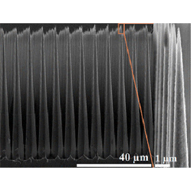
Near-Unity, Unselective Absorption in Sparse InP Nanowire ArraysNP

 
ACS Photonics (2016) 26-Sep-2016 Katherine T. Fountaine, Wen-Hui Cheng, Colton R. Bukowsky, and Harry A. Atwater The article presents experimental results of near-unity broadband (UV-Vis-NIR) and angle-insensitive absorption enabled by optical design of waveguide modes for application in high efficiency, flexible optoelectronic devices.

Enhanced Absorption and <1% Spectrum-and-Angle-Averaged Reflection in Tapered Microwire ArraysNP

 
ACS Photonics (2016) 19-Sep-2016 Sisir Yalamanchili, Hal S. Emmer, Katherine T. Fountaine, Christopher T. Chen, Nathan S. Lewis, and Harry A. Atwater The article studies the favorable optical and electronic properties of tapered silicon microwire arrays fabricated from a bulk silicon wafer via top-down etch procedure.

3D Inkjet printed Ultra-wideband Equi-angular Spiral AntennasNano

 
Proceedings of the IEEE Electronic Components and Technology Conference (ECTC) (2016) 18-Aug-2016 Xing Lan, Maggie Yihong Chen, Xuejun Lu, Wesley Chan, Jun Yu, Neal Yamamoto, May Tan In this paper, we report a flexible 1 to 8 GHz ultra-wideband equi-angular spiral antenna printed using a Fujifilm Dimatix DMP-2831 inkjet printer. The antenna is printed on a 50 μm-thick flexible DuPont Kapton® FPC polyimide film using silver nanoparticle ink. The antenna is measured using an EMSCAN near-field scanner. The measured data proves that the antenna operates over an ultra-wide frequency band from 1 to 8 GHz as designed with excellent axial ratio and radiation patterns across the band.

Ab initio phonon coupling and optical response of hot electrons in plasmonic metalsNESD

 
Physical Review B (2016) 11-Aug-2016 Ana M. Brown, Ravishankar Sundararaman, Prineha Narang, William A. Goddard, III, and Harry A. Atwater Ultrafast laser measurements probe the nonequilibrium dynamics of excited electrons in metals with increasing temporal resolution. Electronic structure calculations can provide a detailed microscopic understanding of hot electron dynamics, but a parameter-free description of pump-probe measurements has not yet been possible, despite intensive research, because of the phenomenological treatment of electron-phonon interactions. We present ab initio predictions of the electron-temperature dependent heat capacities and electron-phonon coupling coefficients of plasmonic metals. We find substantial differences from free-electron and semiempirical estimates, especially in noble metals above transient electron temperatures of 2000 K, because of the previously neglected strong dependence of electron-phonon matrix elements on electron energy. We also present first-principles calculations of the electron-temperature dependent dielectric response of hot electrons in plasmonic metals, including direct interband and phonon-assisted intraband transitions, facilitating complete theoretical predictions of the time-resolved optical probe signatures in ultrafast laser experiments.

Quantum PlasmonicsNESD

 
Proc of IEEE (2016) 4-Aug-2016 Jamie M. Fitzgerald, Prineha Narang, Richard V. Craster, Stefan A. Maier, Vincenzo Giannini Quantum plasmonics is an exciting subbranch of nanoplasmonics where the laws of quantum theory are used to describe light-matter interactions on the nanoscale. Plasmonic materials allow extreme subdiffraction confinement of (quantum or classical) light to regions so small that the quantization of both light and matter may be necessary for an accurate description. State-of-the-art experiments now allow us to probe these regimes and push existing theories to the limits which opens up the possibilities of exploring the nature of many-body collective oscillations as well as developing new plasmonic devices, which use the particle quality of light and the wave quality of matter, and have a wealth of potential applications in sensing, lasing, and quantum computing. This merging of fundamental condensed matter theory with application-rich electromagnetism (and a splash of quantum optics thrown in) gives rise to a fascinating area of modern physics that is still very much in its infancy. In this review, we discuss and compare the key models and experiments used to explore how the quantum nature of electrons impacts plasmonics in the context of quantum size corrections of localized plasmons and quantum tunneling between nanoparticle dimers. We also look at some of the remarkable experiments that are revealing the quantum nature of surface plasmon polaritons.

(Invited Review article) Modeling, simulation, and implementation of solar-driven water-splitting devicesNP

 
Angewandte Chemie (2016) 27-Jul-2016 Dr. Chengxiang Xiang, Dr. Adam Z. Weber, Prof. Shane Ardo, Dr. Alan Berger, YiKai Chen, Prof. Robert Coridan, Dr. Katherine T. Fountaine, Prof. Sophia Haussener, Prof. Shu Hu, Dr. Rui Liu, Prof. Nathan S. Lewis, Dr. Miguel A. Modestino, Dr. Matthew M. Shaner, Prof. Meenesh R. Singh, Dr. John C. Stevens, Dr. Ke Sun, Dr. Karl Walczak The Review focuses on the modeling- and simulation-guided development and implementation of solar-driven water-splitting prototypes from a holistic viewpoint that explores the various interplays between the components.

Impingement Cooled Embedded Diamond Multiphysics Co-DesignNSD

 
Proceedings of the IEEE Intersociety Conference on Thermal and Thermomechanical Phenomena in Electronic Systems (2016) 21-Jul-2016 This paper describes engineering analysis and experimental evaluations used to design an innovative imbedded cooling concept for RF thermal management.The concept, called Impingement Cooled Embedded Diamond(ICED), uses liquid flowing through diamond-lined microchannels etched into the back of a GaN - on - SiC RF die to manage heat produced by the transistors.This approach combines the superior heat spreading of high - conductivity diamond with the outstanding convection capability of impinging jets to manage local heat fluxes as high as 30 kW / cm2.The first part of this paper presents the CFD analysis used to design the microfluidics, select diamond thickness, and understand the sensitivity of performance to component assembly, coolant temperature and composition, and channel dimensions.It also describes the structural analysis used to evaluate ICED mechanical stress levels, including those imposed by diamond growth and hardware assembly.The second part of this paper presents experimental measurements performed to validate the computer models and demonstrate the thermal management capability of the proposed design.These experiments confirmed the effectiveness of the impinging jets at drawing heat produced by the transistors directly to the coolant, reducing transistor mutual heating and enabling a four - fold increase in expected RF output power.They also showed the proposed cooling concept mitigates self - heating thermal limitations and enables aggressive design compaction not possible with existing conduction GaN - on - SiC cooling solutions.

Feasibility of graphene CRLH metamaterial waveguides and leaky wave antennasNP

 
Journal of Applied Physics (2016) 6-Jul-2016 Derrick A. Chu, Philip W. C. Hon, Tatsuo Itoh, and Benjamin S. Williams The feasibility of composite right/left-handed (CRLH) metamaterial waveguides based upon graphene plasmons is demonstrated via numerical simulation. Designs are presented that operate in the terahertz frequency range along with their various dimensions. Dispersion relations, radiative and free-carrier losses, and free-carrier based tunability are characterized. Finally, the radiative characteristics are evaluated, along with its feasibility for use as a leaky-wave antenna. While CRLH waveguides are feasible in the terahertz range, their ultimate utility will require precise nanofabrication, and excellent quality graphene to mitigate free-carrier losses.

Cubic Nonlinearity Driven Up-Conversion in High-Field Plasmonic Hot Carrier SystemsNESD

 
Journal of Physical Chem C (2016) 20-Jun-2016 Prineha Narang, Ravishankar Sundararaman, Adam S. Jermyn, William A. Goddard III, and Harry A. Atwater Surface plasmon resonances confine electromagnetic fields to the nanoscale, producing high field strengths suitable for exploiting nonlinear optical properties. We examine the prospect of detecting and utilizing one such property in plasmonic metals: the imaginary part of the cubic susceptibility, which corresponds to two plasmons decaying together to produce high energy carriers. Here we present ab initio predictions of the rates and carrier distributions generated by direct interband and phonon-assisted intraband transitions in one and two-plasmon decay. We propose detection of the higher energy carriers generated from two-plasmon decays that are inaccessible in one-plasmon decay as a viable signature of these processes in ultrafast experiments.

Plasmonic hot carrier dynamics in solid-state and chemical systems for energy conversionNESD

 
Nanophotonics (2016) 11-Jun-2016 Prineha Narang, Ravishankar Sundararaman, Harry A. Atwater

Towards nanoscale multiplexing with parity-time-symmetric plasmonic coaxial waveguideNP

 
Physical Review B (2016) 27-May-2016 Hadiseh Alaeian, Brian Baum, Vladan Jankovic, Mark Lawrence, and Jennifer A. Dionne We theoretically investigate a nanoscale mode-division multiplexing scheme based on parity-time- (PT ) symmetric coaxial plasmonic waveguides. Coaxial waveguides support paired degenerate modes corresponding to distinct orbital angular momentum states. PT -symmetric inclusions of gain and loss break the degeneracy of the paired modes and create new hybrid modes without definite orbital angular momentum. This process can be made thresholdless by matching the mode order with the number of gain and loss sections within the coaxial ring. Using both a Hamiltonian formulation and degenerate perturbation theory, we show how the wave vectors and fields evolve with increased loss/gain and derive sufficient conditions for thresholdless transitions. As a multiplexing filter, this PT -symmetric coaxial waveguide could help double density rates in on-chip nanophotonic networks.

Embedded Diamond GaN HEMTsNSD

 
2016 CS Mantech Digest (2016) 19-May-2016 Vincent Gambin, Benjamin Poust, Dino Ferizovic, Monte Watanabe, Gary Mandrusiak, Thomas Dusseault

Examples of modern quantum sensing and metrology with new results on photon-added coherent statesQSM

 
Quantum Sensing and Nano Electronics and Photonics XIII (2016) 16-Feb-2016 Jerome Luine ; Anjali Singh ; Bryan Gard ; Jonathan Olson Quantum sensing and metrology is the application of non-classical resources to the measurement of physical quantities with precision or accuracy beyond that allowed by classical physics. For many years non-classical resources such as atomic energy quantization, Josephson Effect, and Quantum Hall Effect have been used to define the fundamental units of time, voltage, and resistance, respectively. In recent years non-classical resources such as quantum squeezing and entanglement have been exploited to expand the range of physical phenomena measured with unprecedented precision or accuracy. We summarize some of the recent research on advanced quantum sensing and metrology and discuss our analyses of photon-added coherent states (PACS) of light. These analyses take into account imperfect photon addition and detection processes and show that PACS enable beyond-classical signal-to-noise ratio for photon counting even in cases where the probability of intended photon addition is 80%. We also show that there remains undiscovered fundamental properties of PACS related to their production and implementation.

Localized fields, global impact: Industrial applications of resonant plasmonic materialsNP

 
MRS Bulletin (2015) 16-Dec-2015 J.A. Dionne, A. Baldi, B. Baum, C.-S. Ho, V. Janković, G.V. Naik, T. Narayan, J.A. Scholl and Y. Zhao From the photoinduced transport of energy that accompanies photosynthesis to the transcontinental transmission of optical data that enable the Internet, our world relies and thrives on optical signals. To highlight the importance of optics to society, the United Nations designated 2015 as “The International Year of Light and Light-based Technologies.” Although conventional optical technologies are limited by diffraction, plasmons—collective oscillations of free electrons in a conductor—allow optical signals to be tailored with nanoscale precision. Following decades of fundamental research, several plasmonic technologies have now emerged on the market, and numerous industrial breakthroughs are imminent. This article highlights recent industrially relevant advances in plasmonics, including plasmonic materials and devices for energy; for medical sensing, imaging, and therapeutics; and for information technology. Some of the most exciting industrial applications include solar-driven water purifiers, cell phone Raman spectrometers, high-density holographic displays, photothermal cancer therapeutics, and nanophotonic integrated circuits. We describe the fundamental scientific concepts behind these and related technologies, as well as the successes and challenges associated with technology transfer.

Electronic modulation of infrared radiation in graphene plasmonic modulatorsNP

 
Nature Communications (2015) 7-May-2015 Victor W. Brar, Michelle C. Sherrott, Min Seok Jang, Seyoon Kim, Laura Kim, Mansoo Choi, Luke A. Sweatlock & Harry A. Atwater All matter at finite temperatures emits electromagnetic radiation due to the thermally induced motion of particles and quasiparticles.Dynamic control of this radiation could enable the design of novel infrared sources; however, the spectral characteristics of the radiated power are dictated by the electromagnetic energy density and emissivity, which are ordinarily fixed properties of the material and temperature.Here we experimentally demonstrate tunable electronic control of blackbody emission from graphene plasmonic resonators on a silicon nitride substrate.It is shown that the graphene resonators produce antenna - coupled blackbody radiation, which manifests as narrow spectral emission peaks in the mid-infrared. By continuously varying the nanoresonator carrier density, the frequency and intensity of these spectral features can be modulated via an electrostatic gate.This work opens the door for future devices that may control blackbody radiation at timescales beyond the limits of conventional thermo - optic modulation.


Emulating Bilingual Synaptic Response Using a Junction-Based Artificial Synaptic DeviceNano

 
ACS Nano () H. Tian, X. Cao, Y. Xie, X. Yan, A. Kostelec, D. DiMarzio, C. Chang, L.D. Zhao, W. Wu, J. Tice, J.J. Cha, J. Guo, and H. Wang

Atomically Thin Femtojoule Memristive DeviceNano

 
Advanced Materials () H. Zhao, Z. Dong, H. Tian, D. DiMarzio, M-G Han, L. Zhang, X. Yan, F. Liu, L. Shen, S.J. Han, S. Cronin, W. Wu, J. Tice, J. Guo, and H. Wang

Atomically thin CBRAM enabled by 2-D materials: Scaling Behaviors and Performance LimitsNano

 
IEEE Transactions on Electron Devices (1900) Zhipeng Dong, Huan Zhao, Don DiMarzio, Myung-Geun Han, Lihua Zhang, Jesse Tice, Han Wang, Jing Guo Aggressively scaled, atomically thin CBRAM cells with extremely low switching current and energy are theoretically studied by three-dimensional (3D) kinetic Monte Carlo (MC) simulations and experimentally realized by using atomically thin 2D materials.

Wafer Scale Synthesis of Thin Film Nanocrystalline Arsenic-Phosphorus via Molecular Beam DepositionNSD

 
Nano letters () Eric P. Young1,2, Junsoo Park1,3,4, Tingyu Bai1, Ryan H. DeBlock1, Mike Lange2, Sumiko Poust2, Jesse Tice2, Clincy Cheung1,2, Christopher Choi1, Bruce S. Dunn1, Mark S. Goorsky1, Vidvuds Ozolins3,4, Dwight C. Streit1, and Vincent Gambin

Zero-static power radio-frequency switches based on MoS2 atomristorsNano

 
Nature Communications () M. Kim, R. Ge, X. Wu, X. Lan, J. Tice, JC Lee, D. Akinwande

Fabrication of Ultra-Thin Si Nanopillar Arrays for Polarization-Independent, Spectral Filters in the Near-IRNP

 
SPIE () Ryan Ng, Julia Greer

Experimental Methods for Efficient Solar Hydrogen Production in Microgravity EnvironmentNP

 
JoVE () Katharina Brinkert, Matthias Richter, Oemer Akay, Janine Liedtke, Thorben Konemann, Michael Giersig, Han-Joachim Lewerenz

Optimizing Photonic Nanostructures via Multi-fidelity Gaussian ProcessesNP

 
NIPS 2018 Workshop () Jialin Song, Yury S. Tokpanov, Yuxin Chen, Dagny Fleischman, Harry Atwater, Yisong Yue

Wideband Curved Patch AntennaERFM

 
META 2019 (2019) V. Radisic, Jimmy Hester, Stéphane Larouche In this paper, we introduce a concept to engineer and extend the bandwidth of patch antennas by controlling and designing substrate thickness profile. This concept was validated by HFSS simulation. A concave patch with sinusoidal substrate height profile shows good simulated return loss from 10 to 20 GHz. Simulated three-dimensional radiation patterns are also shown. This antenna can be fabricated using additive manufacturing.

Receding-horizon multi-objective optimization for disaster responseCA

 
American Control Conference 2018 (1900) K. Lee, S. Martinez, J. Cortes, Robert Chen, Mark Milam

Effective surface impedance of anisotropic surface roughnessERFM

 
2019 APS URSI (2019) V. Radisic and S. Larouche

Characterization of the thermo-optic coefficient of silicon oxynitride using whispering gallery mode optical microcavitiesNSD

 
APL () Andre Kovach, Dongyu Chen, Soheil Soltani, Sumiko Poust, and Andrea M. Armani

Machine Learning Techniques for Stellar Light Curve ClassificationEAC

 
Astronomical Journal (1900) Rachel Thorp, Kevin Tat

Microfluidic Impingement Cooled GaN HEMTsNSD

 
GOMAC 2017 (1900) 1 Ben Poust, 1 Dino Ferizovic, 1 Monte Watanabe, 2 Gary Mandrusiak

Approaching Schottky-Mott limit in van der Waals metal–semiconductor contactNSD

 
Nature Communications (2018) 16-May-2018 Yuan Liu, Jian Guo, Enbo Zhu, Sungjoon Lee, Lei Liao, Mengning Ding, Imran Shakir, Yu Huang, Xiangfeng Duan

Low-contact Barrier in 2H/1T’ MoTe2 in-plane Heterostructure Synthesized by Chemical Vapor DepositionNSD

 
Applied Nano Materials () Xiang Zhang1,‡, Zehua Jin1,‡, Luqing Wang1, Jordan A. Hachtel2, Eduardo Villarreal1, Zixing Wang3, Teresa Ha4, Chandra Sekhar Tiwary1, Jiawei Lai1, Liangliang Dong3, Jihui Yang1, Robert Vajtai1, Emilie Ringe1, Juan Carlos Idrobo2, Boris I. Yakobson1, Jun Lou1, Vincent Gambin4, Rachel Koltun4, Pulickel M. Ajayan1,3,*

Normal dispersion silicon oxynitride microresonator Kerr frequency combsNSD

 
optica () Dongyu Chen, Andre Kovach, Sumiko Poust, Vincent Gambin, Andrea M. Armani Whispering gallery mode (WGM) resonators have proven to be a promising platform for generating Kerr frequency combs, an optical source which has found applications in both basic scientific research and advanced technologies. Here, we demonstrate the generation of frequency combs from SiOxNy microtoroidal resonators. Ultra-high quality (UHQ) factors are achieved in these cavities, which enables parametric oscillations with sub-microwatt thresholds.

Maximizing the Current Output in Self-Aligned Graphene-InAs-Metal Vertical TransistorsNSD

 
Nano Letters () Yuan Liu1,2, Jian Guo1, Enbo Zhu1, Jiming Sheng1, Peiqi Wang3, Vincent Gambin4, Yu Huang1,5 and Xiangfeng Duan3,5 To overcome these limitations, we construct a VFET by using single crystal InAs film as the high conductance vertical channel and self-aligned metal contact as the source-drain electrodes, resulting a record high current density over 45,000 A/cm2 at a low bias voltage of 1 V.

Examining the Transition from Multiphoton to Optical-Field Photoemission from Silicon NanostructuresNP

 
Physical Review Letters () Phillip D. Keathley, Guillaume Laurent, Luis F. Velasquez-Garcia, Franz X. Kaertner

[cf]skyword_tracking_tag[/cf]